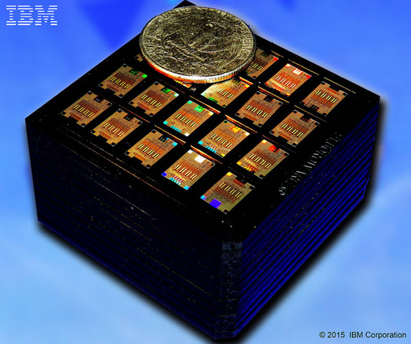
A new breakthrough in the silicon photonics field has been announced by IBM. This is the new fully integrated wavelength multiplexed chip. The new device has been developed to enable the manufacturing of 100Gb/s optical transceivers as well as allow both the electrical and the optical components to be able to be present side by side in the same package.
When it comes to a prolong deployment of optical technology on a short distance, this kind of on-die integration becomes very critical. What is the importance of silicon photonics and why it has taken so long for companies like Intel and IBM to work on it?
Silicon photonics can be the long term replacement of copper
Theoretically, Silicon photonics have the potential to solve some of the big issues that are being encountered with copper interconnection. One of the main problems that is being countered with copper wire it is unable to scale to the level as provided by other parts of the CPU.
![]() After a specific time, it is nearly impossible to make the copper wire any smaller with negotiating on their lifespan or their performance. Theoretically, optical interconnects have the ability to transmit data with less power but the transmission of information will be far quicker.
After a specific time, it is nearly impossible to make the copper wire any smaller with negotiating on their lifespan or their performance. Theoretically, optical interconnects have the ability to transmit data with less power but the transmission of information will be far quicker.
On the other hand, Silicon is a very weak medium when it comes to optical devices. This is mainly because Silicon lacks a band-gap as well as the scale of manufacturing is very different. Relying on Silicon is cost effective when compared to the dependence on other costly mediums like gallium and arsenide.
Despite the slow pace of progress that has been reported by the Silicon photonics, there are many other reasons for the companies to push the technological market to work on this issue. The main reason being that Silicon photonics is most commonly expected to be critical for exascale-level computing.
At present, fiber and copper are used for splitting the transmission market based on the distance. Copper is used between servers or the racks and the Short-run cables but when it comes to long distances fiber becomes more reliable.
![]() The research team of IBM has been able to reduce the node process which is used in the circuit design. At present, there has been no official announcement from IBM pertaining to the release of on-chip silicon photonics based on devices in the near future. But the actual work process of the technology can be very much figured out. This cutting edge technology designs will put the optical components on the similar package as that off of the CPU. This can also be at the edge of the motherboard. This is the main reason why the technology is being considered important for server-to-server linkages as well as for the peripheral connection. These silicon photonics based products are expected to be rolled out on HPC as well as the scientific computing industries. Lots of progress is occurring in the field of silicon photonics. Even though the rolling out of the devices might take some time, but the future of computing looks to be very bright.
The research team of IBM has been able to reduce the node process which is used in the circuit design. At present, there has been no official announcement from IBM pertaining to the release of on-chip silicon photonics based on devices in the near future. But the actual work process of the technology can be very much figured out. This cutting edge technology designs will put the optical components on the similar package as that off of the CPU. This can also be at the edge of the motherboard. This is the main reason why the technology is being considered important for server-to-server linkages as well as for the peripheral connection. These silicon photonics based products are expected to be rolled out on HPC as well as the scientific computing industries. Lots of progress is occurring in the field of silicon photonics. Even though the rolling out of the devices might take some time, but the future of computing looks to be very bright.

 Why Your Link Building Efforts Might Fail
  How to Request or Give Remote Control in a FaceTime Call on iPhone
  The Rise of Intelligent Automation in Business Operations
  The Best Ideas for Designing Your Custom Printed Ring Binder
  How Technology is Changing the Way We Play Hearts
  The Rise of Open Source: A Journey to Innovation and Collaboration
  How SD-WAN Is Revolutionizing Business Networks
  Effective Digital Advertising Strategies for Modern Businesses
  Tips for Marketing Dental Packages: Easy Ways to Grow Your Reach